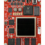

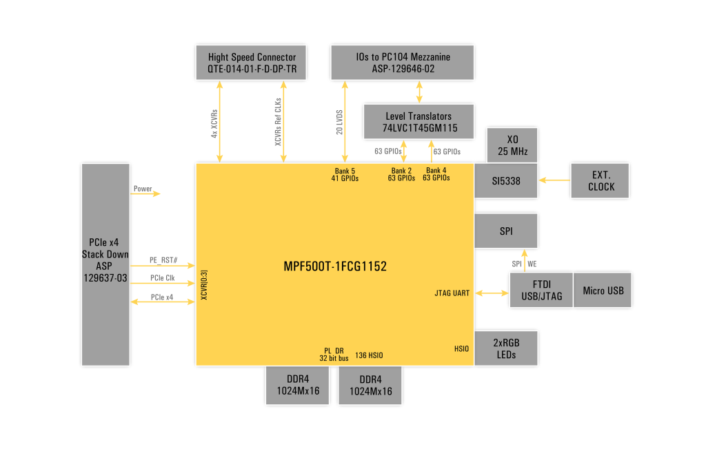
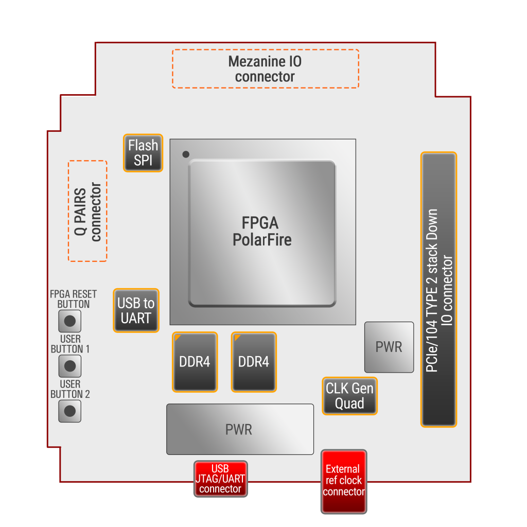
The PCIe104N is a rugged, compact, and highly efficient solution built for demanding industrial/defense environments. Powered by the versatile Microchip PolarFire FPGA MPF500T-1FCG1152I, with an option for the MPF300T-1FCG1152I, this board offers low power consumption without sacrificing performance. Designed in the PCIe104 format, it boasts a 4-lane PCIe interface to the host, perfect for connecting to stack-down hosts and mezzanine cards. Its industrial-grade components, including two DDR4 chips for RAM and external SPI flash for data storage, ensure reliability in demanding applications. With a power input of just 5V and 12V, the PCIe104N keeps power consumption to a minimum while delivering exceptional processing capabilities.
In addition to its small form factor, the PCIe104N is engineered for high expandability and versatility. It features 104 IO signals routed to the mezzanine connector, with 63 5V IOs and 20 LVDS differential pairs, offering flexible options for connecting external peripherals. The onboard Samtec connector provides access to additional transceivers, GPIO, and reference clocks. With robust features like tactile buttons, power-good LEDs, and user-configurable RGB LEDs, this board is optimized for user interaction and system status monitoring. Designed for industrial and military-grade applications, it ensures long-term stability and reliability even in the harshest environments.
Features
- Main FPGA MPF500T-1FCG1152I PolarFire FPGA from Microsemi (now Microchip)
- Option to assemble with an MPF300T-1FCG1152I device.
- Module is in PCIe104 format with 4 lanes of PCIe interface to host
- Module has a connection to the stack down host.
- It is be able to connect to a PCIe104 format host, via a stack down connection and on the other side of the card it fits to a custom mezzanine card.
- 104 IO signals routed to the mezzanine connector (ASP-129637-02)
- Samtec QTE-014-01-F-D-DP-TR connector for accessing 4 additional transceivers, 1 pair of GPIO, clock capable I/Os, and reference clocks.
- Module only boots from the internal NVM FLASH for enhanced security
- For additional security there is a restriction on writing to or modifying the content of the external SPI FLASH and the internal NVM FLASH from the host interface. Only through JTAG, the flash content can be modified.
- Three tactile buttons, two for the user, and one reset button.
- FLASH can be accessed for write operation through JTAG only.
- Four power good LEDs, Two User RGB LEDS.
- The module uses industrial grade components.
- Two industrial grade DDR4 chips for RAM organized as 32-bit bus.
- External SPI Flash for user data storage only.
- Input power 5V, 3A max. 12V – for fan only.
Applications
- Defense
- Medical Imaging
- Machine Vision
- Stereo vision
- Artificial Reality /Augmented Reality
- Control
- Instrumentation and testing
- Data capture and logging
PCIe104N block diagram
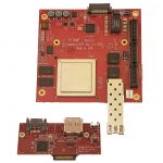
PCIe104Z Placement Diagram
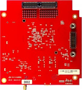
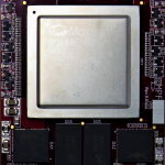
Solder side of PCIe104Z
- PCIe104N-MPF500-I
- PCIe104N-MPF300-I
Extended temperature and other speed grades available with MOQ, contact Sundance support for more information